About this HTML presentation
This Shipslides page presents Nanotechnology / Engineering at the atomic scale as an interactive HTML presentation deck in the Technology catalog with 13 slides. The share page keeps the uploaded deck sandboxed while exposing readable context, topics, and a slide outline for viewers and search engines.
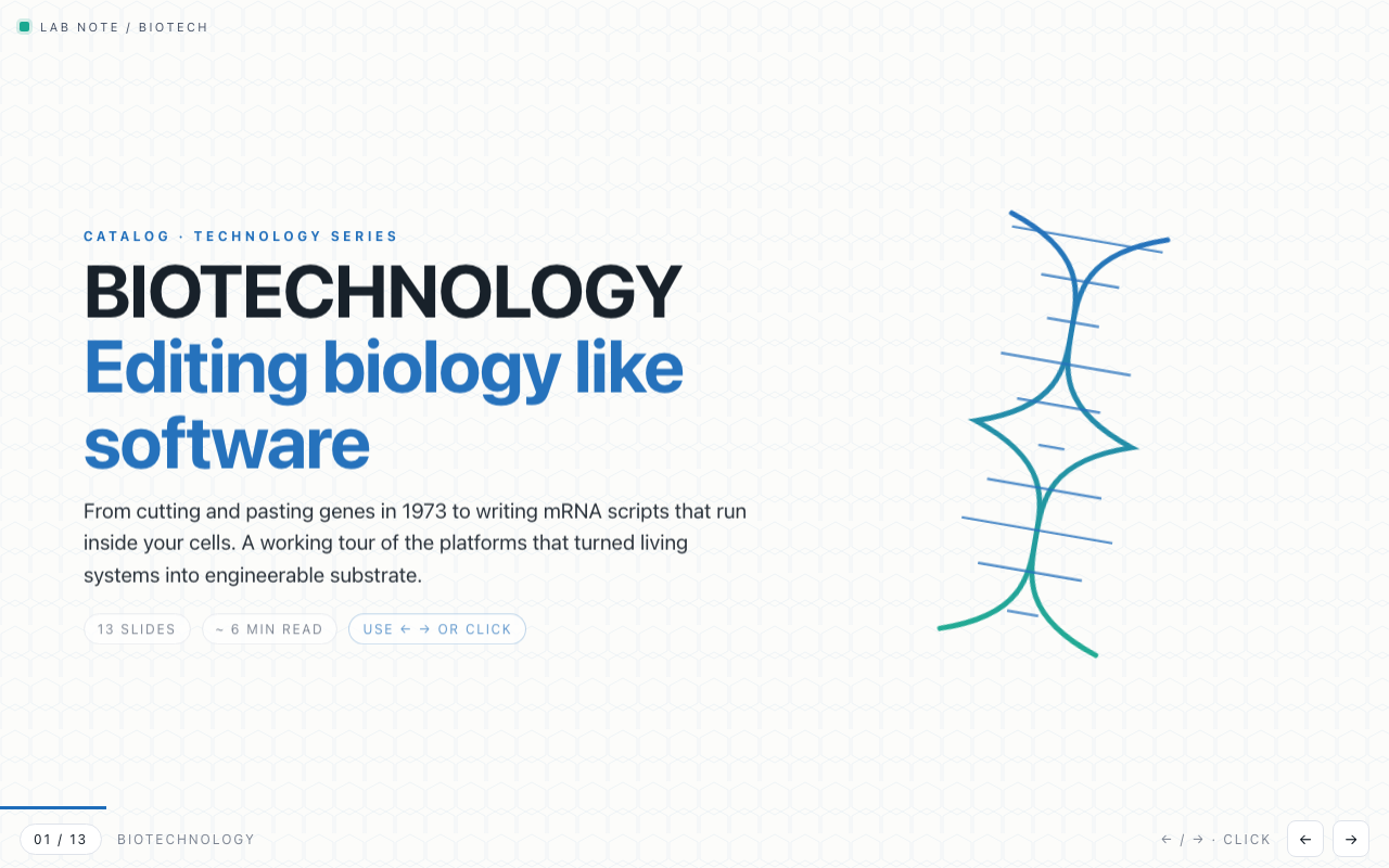
Caltech, December 29, 1959 . Richard Feynman delivers the founding lecture of nanotechnology before the field exists. Key sections include: NANO TECH / NOLOGY; "Plenty of Room at the Bottom"; One nanometer is vanishingly small.; Scanning Tunneling Microscope / 1981; "IBM" in xenon atoms / 1989; A rolled sheet of graphene / 1991; One atom thick / 2004; Chemistry does the building for you.; Where nano already ships.; Patterning silicon at the atom limit..
Key sections
- 01NANO TECH / NOLOGY
- 02"Plenty of Room at the Bottom"
- 03One nanometer is vanishingly small.
- 04Scanning Tunneling Microscope / 1981
- 05"IBM" in xenon atoms / 1989
- 06A rolled sheet of graphene / 1991
- 07One atom thick / 2004
- 08Chemistry does the building for you.
- 09Where nano already ships.
- 10Patterning silicon at the atom limit.
- 11Toxicology hasn't caught up.
- 12What nano is , and isn't.
- 13Where to go next.